 13 January,2022
 By Aovxers
 AOVX hardware workshop
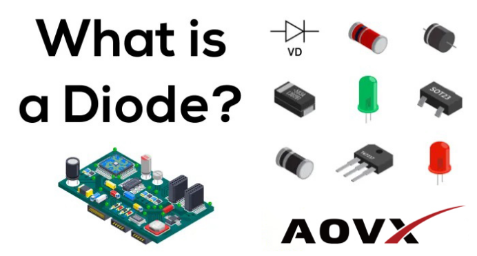
A diode is one of the most commonly used electronic components. Its biggest characteristic is unidirectional conduction, that is, current can only flow in one direction of the diode. The function of the diode includes a rectifier circuit, detection circuit, voltage regulator circuit, and various modulation circuits. , mainly composed of diodes; It is because of the invention of diodes and other components that our present colorful electronic information world was born.
Asset monitoring device under IoT technology is also an inseparable diode, AOVX tracker solutions is a logistics visualized supply chain management solution provider focusing on the field of wireless communication.

Goods monitoring

Assets tracking
Vehicle tracking

Environmental monitoring
Introduction to Diode Devices
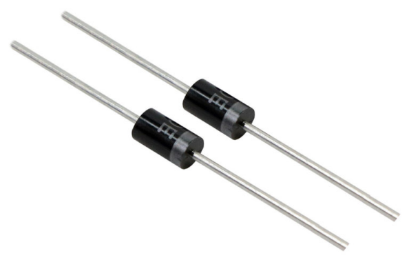
Most relevant to diodes is the ability to conduct electricity in one direction.
A diode is different from linear passive devices such as resistors, capacitors and inductors because it is a semiconductor device and is nonlinear, with the characteristics of PN junction (volt-ampere characteristics); it is also not like semiconductor devices such as transistors and field effect transistors, because it It is a passive device and can realize the function of the device without external power supply.
Learn the formation of PN junction
The PN junction is formed by the diffusion motion of majority carriers and the drift motion of minority carriers.
The formation of PN junction: The holes (positively charged) in the P region and the free electrons (negatively charged) in the N region in the left image of Figure 11-1 can move. And the negative ions in the P region and the positive ions in the N region are fixed. Due to the diffusion motion, holes and free electrons recombine, forming a space charge region, shown on the right. Due to the continuous increase of the charge region, the internal electric field increases. Under the action of the electric field force, drift motion occurs, so that the fixed negative ions in the space charge region on the side of the P region attract the holes in the N region (repel the holes in the N region). Free electrons); also make the fixed positive ions in the space charge region on the side of the N region attract the free electrons in the P region (repel the holes in the P region), so as to achieve dynamic equilibrium and make the space charge region reach a fixed width. This fixed space charge region is the PN junction, shown on the right of Figure 11-1.
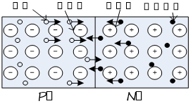
Figure 11-1
Forward conduction and reverse cutoff
The positive applied voltage is applied to the PN junction to make it conduct (P pole is connected to the positive power supply, N pole is connected to the negative power supply), and the majority carrier flows to generate a positive conduction current.
The reverse applied voltage PN junction is cut off (the N pole is connected to the positive of the external power supply, and the P pole is connected to the negative of the external power supply), and the minority carriers flow to form a reverse current.
When a forward voltage is applied to the PN junction, the applied electric field force is opposite to the internal electric field force, which narrows the space charge region. When the applied electric field force is applied to a certain level, it just overcomes the internal electric field force (for example, the applied voltage reaches 0.6V), at this time, the diffusion movement is intensified, a forward current is formed, and the PN junction is turned on.
When a reverse voltage is applied to the PN junction, the applied electric field force is consistent with the internal electric field force, which widens the space charge region. In this way, the internal electric force increases, further preventing the flow of current. However, due to the drift motion of very few minority carriers, a very small reverse current is generated.
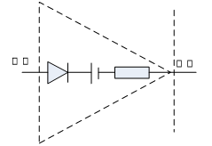
Figure 11-2
Figure 11-2 is the schematic diagram of the diode after PN junction package. The dynamic resistance in series is added in the figure. This resistance is the resistance value R(d) of the pin of the diode. If the applied voltage is directly connected to both ends of the diode to make it positive After the conduction (there is no current limiting resistor), the current will continue to increase, then this resistor will generate thermal power dissipation, and when the current increases to a certain value, the R(d) will be burned due to overheating, resulting in damage to the diode.
²Use silicon tube or germanium tube?
As shown in Table 11-1 below, the germanium tube has a smaller on-state voltage drop than the silicon tube, but the silicon tube has a smaller reverse current than the germanium tube, and the silicon tube has better stability at high temperature.
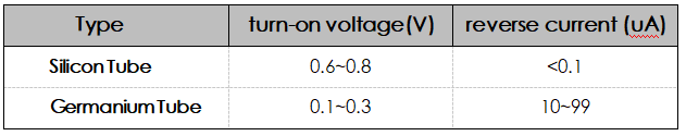
Sheet 11-1
In the analog circuit, when we analyze or design the circuit, we must first determine whether the tube is a silicon tube or a germanium tube, and judge according to the VF (forward voltage drop) parameter in the diode specification. Sometimes the difference of 0.1V will The design of the circuit is abnormal.
Forward voltage drop and reverse current
Both the forward voltage drop and reverse current of a diode are affected by temperature. For every 1°C increase in temperature, the forward voltage drop decreases by 2.5mV; for every 10°C increase in temperature, the reverse current approximately doubles. Figure 11-3 is the volt-ampere curve of the diode. It can also be seen in the figure that as the temperature increases, the forward characteristic curve of the diode shifts to the left; the reverse characteristic curve of the diode shifts downward.

Figure 11-3
The following are two cases to illustrate the effect of temperature change on the forward voltage drop and reverse current of the diode.
Case 1: Forward Current
Remember the design modification we swapped out of the Zener for one or more forward-biased series diodes in our discussion of the voltage regulator circuit where the transistor introduces feedback? So the forward bias voltage drop of the diode is the Vz we need. Therefore, if we use a diode as the bias, if the temperature changes at 40°C, it will cause a change in the bias voltage of 2.5mVx40=100mV, which will cause a voltage error in the output of the regulated power supply.
Case 2: Reverse Current
Assuming a germanium tube, the reverse current at 25°C is 100uA, when the temperature rises to 35°C, the reverse current is 200uA; when the temperature continues to rise to 75°C, the reverse current is 3.2mA. In this way, not only the unidirectional conduction performance of the diode is violated (because it is impossible for a large current to flow in the reverse direction during normal use), but the tube is easily damaged by overheating.
Key selection parameters of diodes
Generally, the diodes we often use in circuit design are: common detection diodes, rectifier diodes with high reverse peak voltage, Schottky diodes with low voltage drop, and zener diodes with various powers.
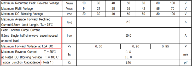
Figure 11-4
Referring to Figure 11-4, when selecting models, we need to focus on the following parameters when selecting models.
1. Reverse peak voltage, this parameter is to investigate whether the applied reverse voltage will break down and damage the diode when the diode is turned off in reverse.
2. Maximum forward current and peak current. This parameter is the current value that is allowed to flow when the diode is forward biased and turned on. If it is too large, the diode will be damaged by heat.
3. Maximum reverse current: This parameter can reflect the unidirectional conductivity of the diode. The smaller the reverse current, the larger the reverse resistance and the better unidirectional conductivity. At the same time, the excessive reverse leakage current will also bring some circuits. trouble. But for Zener diodes, this parameter is not a bad thing.
4. Forward voltage drop: This parameter expresses the forward voltage drop. For example, when it is used for the power isolation circuit mentioned below, it is hoped that the smaller the forward voltage drop, the less it will affect the power supply voltage to the load. Therefore, the value of ordinary diodes is 0.7V~1.5V, while Schottky tubes can reach below 0.5V.
Learn more about AOVX :
The wireless sensor monitoring technology developed by the AOVX creatively integrates the three elements of “people”, “goods” and “warehouses” in the logistics supply chain into one platform, and conducts all-around data collection and analysis for personnel, goods, and the environment in warehousing and logistics monitor.
Website: www.aovx.com
Email: info@aovx.com
Interest in more solutions? follow us at Linkedin:
https://www.linkedin.com/company/aovxassetstracker/mycompany/?viewAsMember=true


Latest Posts
Categories


