 10 February,2022
 By Aovxers
 AOVX hardware workshop
In Aovx's asset monitoring device, diodes are often used. In the previous discussion, the types and functions of diodes were also introduced.
Click: https://www.aovx.com/News.html ,Learn more about diodes.

As a logistics visualized supply chain management solution provider focusing on the field of wireless communication. Generally , in the Aovx asset monitoring device, the diode is the core component of the integrated circuit and can also amplify the signal.
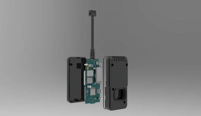
For example, Aovx's V-series, vehicle tracking devices are mainly used in fleet management business.
The Features included :
Motion Detect
Vibration Alert
Electronic Fence
Tamper Alert
Low Battery Alert
ACC ON OFF Detection
GPIOs
But the features function design can not do without diode , if you have more interested in this ...Lets learn the Common circuit design of diodes immediately
Logic isolation circuit
The diode can pass the one with the higher input voltage in the circuit, but does not affect the one with the lower input voltage; it not only has the function of logical OR, but also has the function of multi-channel isolation.
As can be seen from Figure 14-1, the voltage of the USB interface of the computer is about 5V. When the USB and the power adapter are powered at the same time, the 5.5V voltage of the adapter will not affect the 5V of the computer's USB (the high voltage will not be serialized into the USB). Voltage; in the same way, when the voltage of the adapter is 4.5V, the 5V power supply voltage of the USB will not have any effect. In addition, the adapter and USB can also work independently, and the diode here generally chooses a power Schottky diodes (the forward voltage drop is generally small, generally about 0.4V).
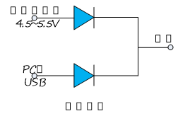
Figure 14-1
When performing digital signal transmission, it is often encountered that the digital voltage domain of the GPIO is different. For example, when a 3V MCU communicates with a 5V MCU through serial port, in order to prevent the interface of the 3V MCU from being damaged by the 5V voltage, the direct connection method cannot be used. At this time, it can be level-shifted with a diode (transistor and MOS diodes design will also be used).
In Figure 14-2, A and B are connected to two interfaces of different voltage domains respectively, and the B terminal is set to a low level, so that the diode is forward-conducting, and the left A terminal is clamped at about 0.6V (specifically Look at the turn-on voltage parameters of the diode used), while the logic level of 0.6V for the 3.3V voltage domain is a low level, that is, the A terminal also appears as a low level.
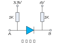
Figure 14-2
When the B terminal is set to a high level (5V), since the cathode potential of the diode is higher than the anode potential, the diode is turned off, so the voltage of the A terminal is set to a high level (3.3V) by the 1K resistor.
Inductive load protection circuit
Since the inductive device has a very important characteristic, that is, the current cannot be abruptly changed, so it is necessary to add a freewheeling loop to it. Due to the sudden opening of the originally closed switch in the left picture of Figure 14-3, the current path flowing through the inductive device changes instantaneously, and the current will pass through the surrounding air to form a current loop. However, the impedance of the air is very large, so the current flowing through the air will generate a very large high voltage, resulting in sparks. If a triode or a MOS diodes is used as a switch, such a high voltage can easily damage the switch diodes.
In the right picture of Figure 14-3, the diode is used to freewheel the current when the switch is turned off, thereby preventing the sudden change of the current of the inductive device and causing high voltage damage to the switch diodes.
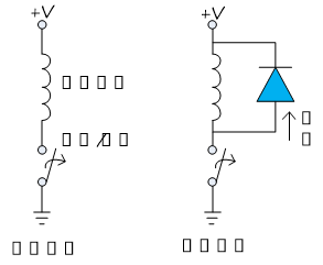
Figure 14-3
Clamp Limiter Circuit
The clamp circuit on the left side of Figure 14-4 limits the output signal between -5.6V and +5.6V. It is required here that the reverse breakdown voltage of the diode must be greater than 10.6V. This circuit is a standard protection circuit at the input end of CMOS series digital logic circuits, which needs to protect the interface from electrostatic damage.
The limiter circuit in the figure on the right limits the output signal to ±0.6V. This circuit is mainly used for input protection of high gain amplifiers.
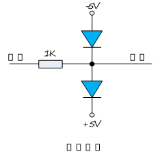
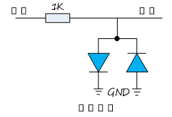
Figure 14-4
Detection is to use the unidirectional conductivity of diodes to obtain unipolar waveforms. If the input signal is a sine wave, we can also regard it as a rectification process, such as the rectification application of diodes in power supplies.
In the left side of Figure 14-5, the input pulse signal passes through a differentiator composed of C and R1, so that the edge signal of the input pulse signal is allowed, and after passing through the detector composed of D and R2, the output is greater than 0.6V. signal (the forward voltage of the diode is set to 0.6V), so that an edge corresponds to a pulse. But this kind of circuit is not suitable for the input signal whose peak-to-peak value is less than 0.6V, because there is no output.
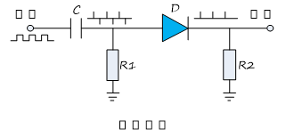
Figure 14-5
Therefore, to address the functional limitations imposed by the diode forward voltage drop (0.6V), Figure 14-6 implements a detection circuit that compensates for the forward voltage drop. Using D1's clamping and limiting feature, R3 and D1 always provide a DC bias of 0.6V for D, so that D will always remain on. In this way, even the input signal less than 0.6V can pass through D unimpeded. In particular, when the temperature changes, the forward voltage drop of D1 and D will change at the same time, so that D1 can also compensate for the temperature change.
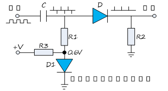
Figure 14-6
Rectifier circuit
Figures 14-7 and 14-8 show the circuits and waveforms of diode half-wave rectification (left) and full-wave rectification (right), respectively.
The input is an AC voltage of 50Hz, and there is no capacitor for filtering and storage after rectification. In this way, the output of half-wave rectification is still the AC voltage waveform of 50Hz, but the lower half of the AC input is cut off; the output of full-wave rectification is the AC voltage waveform of 100Hz, and the lower half of the AC input is also rectified and output by the diode path. .
Comparing the input and output waveforms, it can be seen that the diode needs to withstand a peak voltage when there is no back-end capacitor.
The diode needs to withstand twice the peak voltage when there is a back-end capacitor
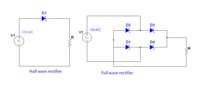
Figure 14-7
In Figure 14-8, the blue curve is the 10VAC waveform, and the red curve is the rectified output waveform. We can also see that for the input, the output voltage has a diode drop.
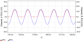
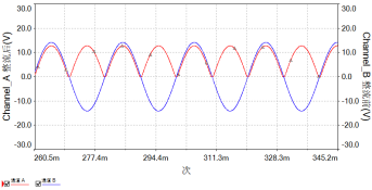
Figure 14-8
Regulator circuit
The DC positive and negative power supply voltage regulator circuit shown in Figure 14-9. In the figure, a Zener diodes is used to output positive and negative voltages at the same time. If the GND in D5 and D6 is removed, and the negative pole is connected to GND, then the circuit is a positive voltage power supply that outputs 2Vz.
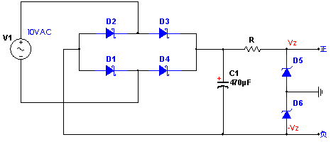
Figure 14-9
Voltage delay translation circuit
As shown in Figure 14-10, when the voltage Vin is input, the voltage regulator diodes will not be in a breakdown state until the voltage reaches Vz, or when the voltage of VRC reaches Vz, Vout will start to have voltage output, and at the same time change with the input voltage, but The output voltage is always Vz lower than the input voltage.
Starting from Vin input, the time delay in the time period when the VRC voltage has not reached the Vz value is determined by the values of Rin and Cin.
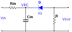
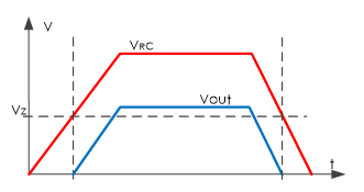
Figure 14-10
Learn more about AOVX :
The wireless sensor monitoring technology developed by the AOVX creatively integrates the three elements of “people”, “goods” and “warehouses” in the logistics supply chain into one platform, and conducts all-around data collection and analysis for personnel, goods, and the environment in warehousing and logistics monitor.
Website: www.aovx.com


Latest Posts
Categories


